情報と価格についてはお問い合わせください
専門家のアドバイスと研究ニーズに合わせたソリューションを入手してください
2026年11月18日
See the Surface at the Atomic Scale
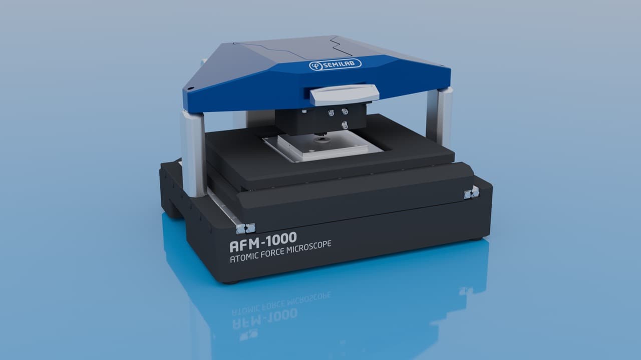
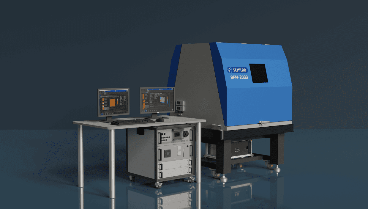
Although a wafer’s surface may look smooth to the naked eye, tiny height variations can greatly affect the devices built on it. Semilab’s Atomic Force Microscopy (AFM) creates highly detailed 3D maps of wafer surfaces, helping researchers and manufacturers characterize the surfaces of silicon, silicon carbide and gallium nitride samples.
A Closer Look at Every Contour
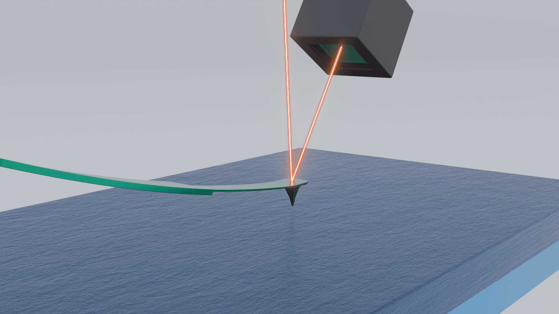
AFM uses a sharp tip to probe the sample surface and records the surface height as the tip moves. The result is a 3D topography map that reveals surface texture, roughness and fine features, including steps just a few atoms high.

Turning Surface Texture into Useful Numbers
Roughness parameters summarize surface-height variations in a form that can be compared between samples or process steps. One common measure is Ra, the average absolute deviation of the surface from its mean height over the measured area or profile.

Ra gives a useful overall picture, but a single number cannot describe every characteristic. A topography map or profile can also reveal local details such as terraces, step bunching and other surface structures.
Why Surface Roughness Matters
Surface texture can influence how materials and layers interact. In semiconductor devices, for example, the interface between the substrate and gate dielectric can affect transistor mobility. Measuring roughness helps teams characterize wafer quality and better understand these important interfaces.
Surface Insight for Different Wafer Types
AFM can characterize surface roughness parameters in Si, SiC and GaN wafers across a range of conditions and structures including annealed, epitaxial, polished, unpolished and SOI samples. From an overall roughness value to fine surface features, AFM helps make wafer topography measurable and comparable.
Interested in surface characterization? Check out our infographic!
https://semilab.com/en/news/pushing-size-limits-in-the-semiconductor-industry-and-metrology