歡迎洽詢產品資訊與報價
針對您的研究需求,提供專業諮詢與客製化解決方案
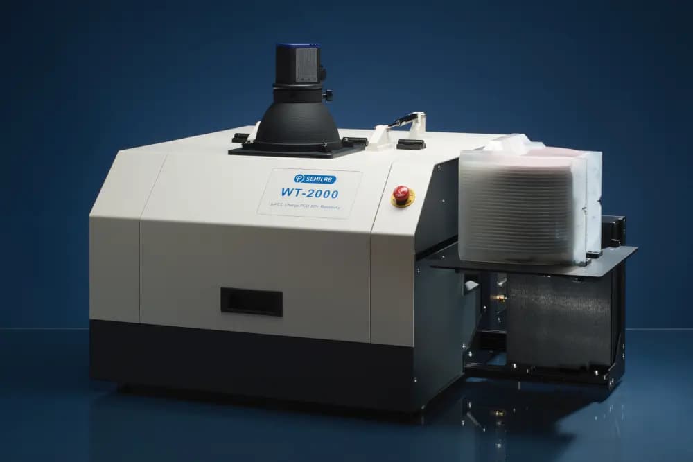
MeV H+或He+植入CZ-Si中設定載子壽命,以達到功率元件的客製化。 商用微波光電導衰減(μ-PCD,Semilab, Inc.)設備旨在用於晶圓表徵。 µ-PCD 資料的實際評估需要一個模型來處理偵測載具口袋與所需缺陷分佈不符的情況。 此多層模型的參數是使用 TRIM 程式碼從空位分佈中提取的。
N.Q. Khanh, P. Tüttő, E.N. Jaroli, O. Buiu, L.P. Bíró, F. Pászti, T. Mohácsy, Cs. Kovacsics, A. Manuaba, J. Gyulai
See our related products to this publication: