联系我们获取详情与报价
获取专家建议,为您研发需求量身定制解决方案
2026年10月27日
The Growing Complexity of Advanced Packaging
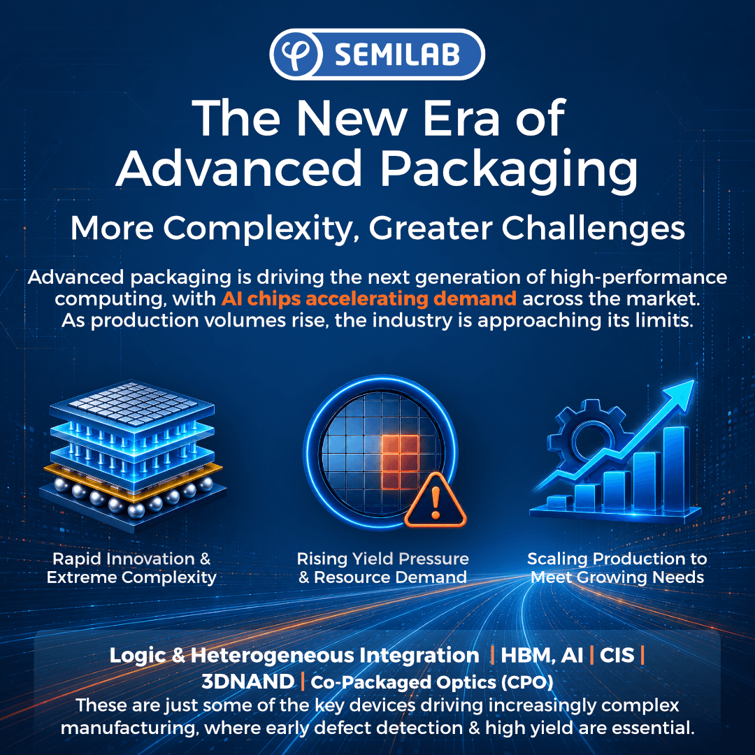
The rapid development of artificial intelligence (AI) and high-performance computing (HPC) is transforming semiconductor manufacturing. As demand for higher computational performance, greater memory bandwidth and improved energy efficiency continues to grow, advanced semiconductor packaging technologies are becoming increasingly important.
From heterogeneous integration and High Bandwidth Memory (HBM) to CMOS Image Sensors (CIS), 3D NAND and Co-Packaged Optics (CPO), increasingly sophisticated device architectures are introducing new challenges across semiconductor manufacturing.
Greater process complexity, tighter tolerances and growing production volumes place increasing pressure on manufacturers to maintain consistently high yields. At the same time, rising demand for energy, water and other resources reinforces the importance of manufacturing efficiency.
Meeting these challenges requires more than expanding production capacity. Early detection of process variations, precise material characterization and reliable process control are essential for maintaining manufacturing quality and efficiency.
Advanced packaging metrology provides the measurement capabilities needed to address these requirements, enabling manufacturers to better understand critical process parameters and optimize production processes.
Hybrid Bonding: Where Precision Becomes Critical
Hybrid Bonding demonstrates how increasingly complex semiconductor packaging technologies are driving the need for more precise measurement and process characterization.
By combining direct dielectric-to-dielectric bonding with metallic interconnect bonding, Hybrid Bonding enables high-density interconnections and supports increasingly sophisticated semiconductor architectures. However, achieving reliable bonding requires tightly controlled wafer geometry, thin-film properties and surface conditions.
Variations in wafer thickness, bow/warp, material composition or surface topography can influence alignment accuracy, bonding quality and final device performance.
Reliable Hybrid Bonding process control therefore depends on selecting the appropriate metrology technique for each critical parameter. Identifying and understanding these variations at different manufacturing stages helps manufacturers optimize processes and reduce the risk of defects affecting subsequent production steps.
Complementary Metrology Solutions for Advanced Packaging
As advanced packaging manufacturing becomes more demanding, no single measurement technique can provide a complete understanding of every critical process parameter.
The Semilab advanced packaging portfolio brings together complementary optical and electrical metrology solutions, alongside high-resolution surface characterization, to support critical measurement applications throughout semiconductor manufacturing.
Wafer Geometry and Dimensional Characterization
Precise wafer geometry measurement is particularly important in advanced packaging processes that require accurate alignment and uniform bonding conditions.
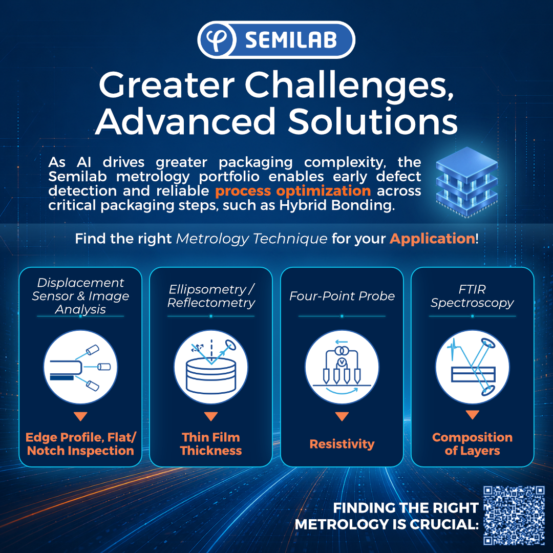
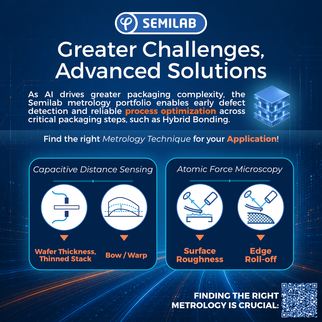
Capacitive Distance Sensing enables wafer thickness and bow/warp characterization, providing insight into dimensional variations that can affect process stability and bonding uniformity.
Displacement Sensor and Image Analysis techniques support wafer edge profile characterization, including flat and notch inspection. These measurements help manufacturers evaluate geometrical features relevant to wafer handling, positioning and process control.
Thin-Film Thickness and Material Characterization
Thin-film thickness and material composition are critical parameters in advanced packaging, influencing process consistency and the properties of functional layers.
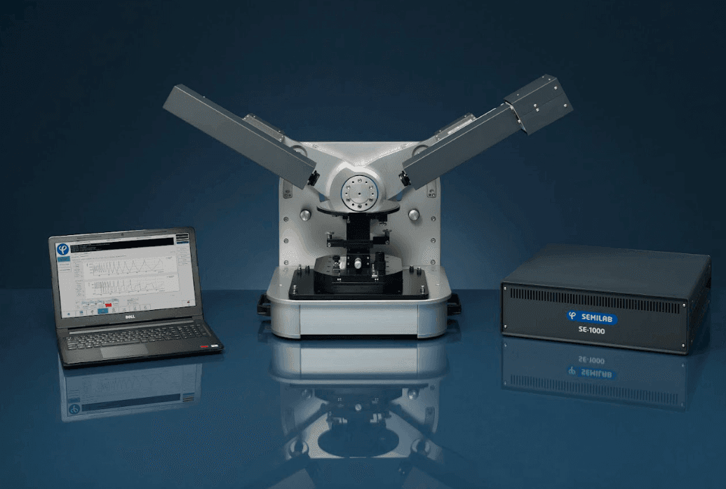
Ellipsometry and Reflectometry enable optical thin-film thickness measurement, supporting the monitoring of layer uniformity and deposition processes.
Fourier Transform Infrared (FTIR) Spectroscopy provides information about material composition through infrared absorption characteristics, supporting layer identification and process characterization.
Together, these optical metrology techniques help manufacturers detect variations in thin-film properties and gain better control over critical manufacturing steps.
Electrical Properties and Resistivity Measurement
Electrical metrology complements optical and dimensional characterization by providing insight into the properties and uniformity of conductive materials.
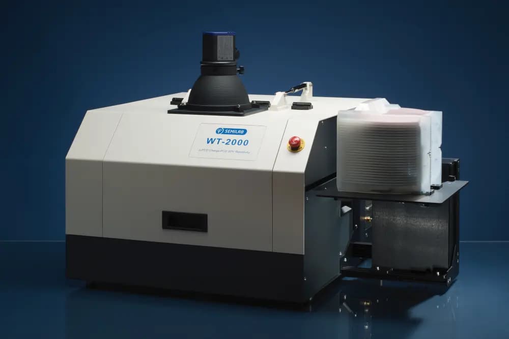
Four-Point Probe (4PP) measurements enable electrical resistivity characterization, helping manufacturers evaluate material uniformity and identify variations relevant to semiconductor process optimization.
Surface Topography and Roughness Characterization
Surface quality is particularly important in Hybrid Bonding, where bonding performance depends on precisely controlled surface conditions.
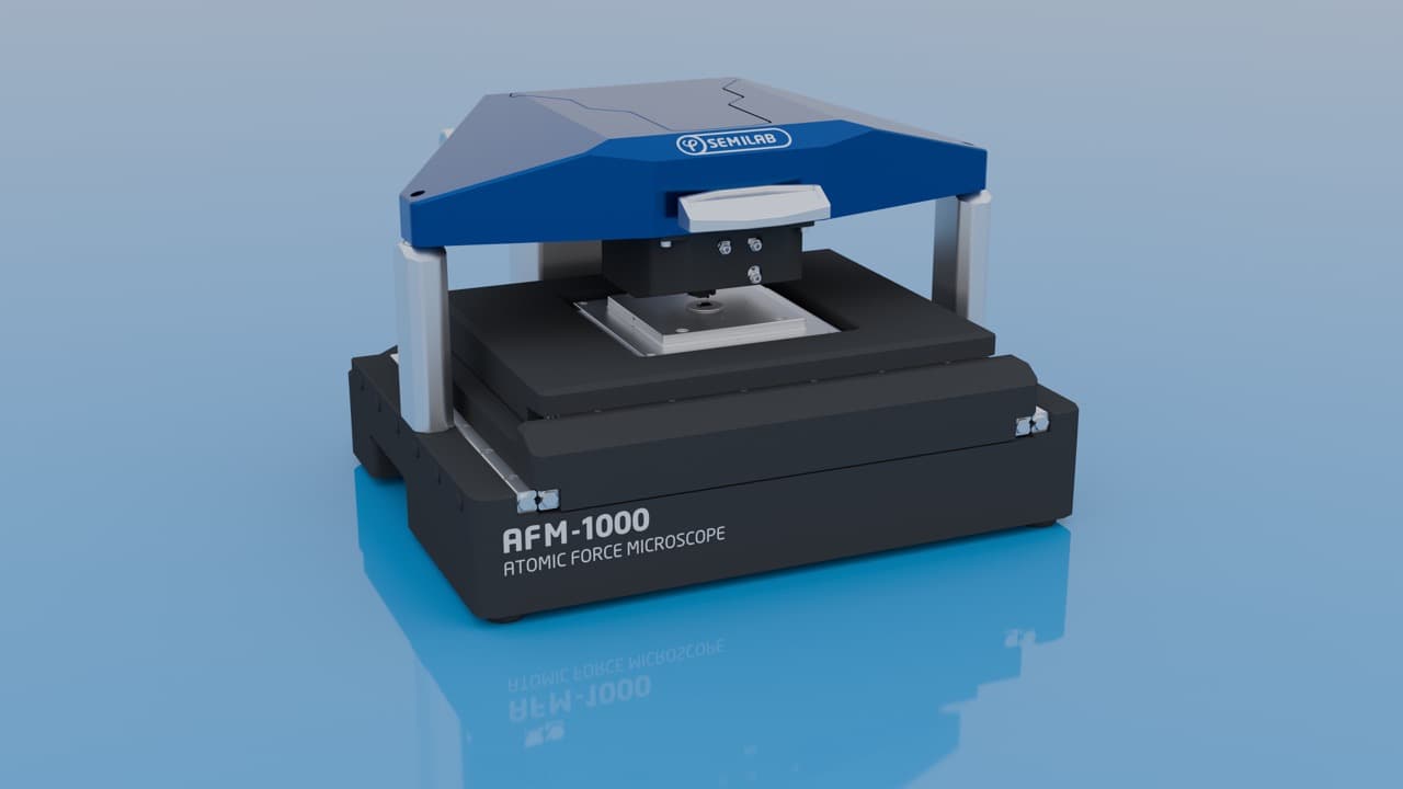
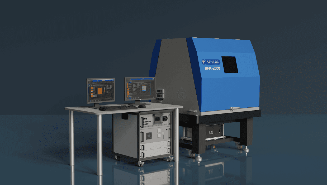
Atomic Force Microscopy (AFM) provides high-resolution surface topography measurements, including surface roughness and edge roll-off characterization.
By identifying local surface variations, AFM supports the evaluation of bonding surfaces and the optimization of surface preparation processes.
 From Measurement Data to Reliable Process Control
The value of advanced semiconductor metrology extends beyond individual measurements. Understanding how wafer geometry, thin-film properties, electrical characteristics and surface conditions influence manufacturing outcomes is essential for maintaining product quality and yield.
Selecting the appropriate metrology technique for each application enables manufacturers to identify process deviations earlier, better understand manufacturing variations and make more informed process optimization decisions.
As advanced packaging technologies evolve toward higher integration densities and tighter manufacturing tolerances, reliable measurement data becomes increasingly important for maintaining process stability and supporting efficient production.
Supporting the Future of Advanced Packaging
As AI-driven demand continues to accelerate semiconductor innovation, advanced packaging will remain essential for enabling higher-performance, more energy-efficient devices.
Technologies such as Hybrid Bonding highlight the growing importance of precise characterization and reliable process control throughout the semiconductor manufacturing process.
With complementary optical, electrical and surface characterization capabilities, the Semilab advanced packaging portfolio supports manufacturers in understanding critical process variations, optimizing manufacturing processes and maintaining reliable process control as device complexity increases.
Explore the Semilab Advanced Packaging portfolio and find the right metrology solution for your application.