
联系我们获取详情与报价
获取专家建议,为您研发需求量身定制解决方案
2026年8月11日
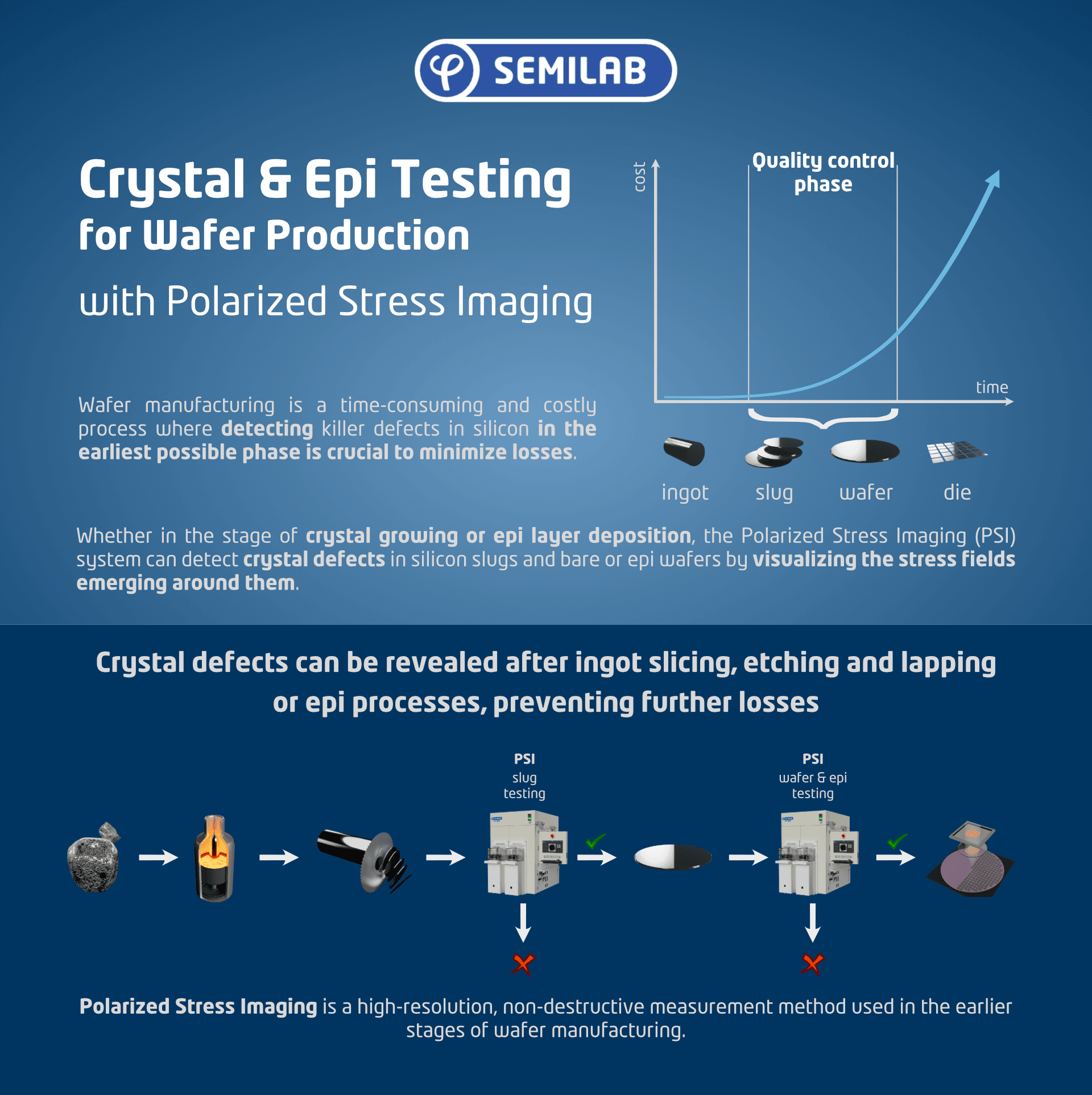
Wafer manufacturing is a time-consuming and costly process, where detecting killer defects in silicon (Si) in the earliest possible phase is crucial to minimize losses. To minimize losses, it is crucial to detect killer defects in silicon in the earliest possible phase.
Polarized Stress Imaging is a high-resolution, non-destructive measurement method used in the earlier stages of wafer manufacturing. Whether in the stage of crystal growing or epi layer deposition, the Semilab Polarized Stress Imaging (PSI) system was designed to be able to detect crystal defects in Si and bare or epi wafers by visualizing the stress fields emerging around them.
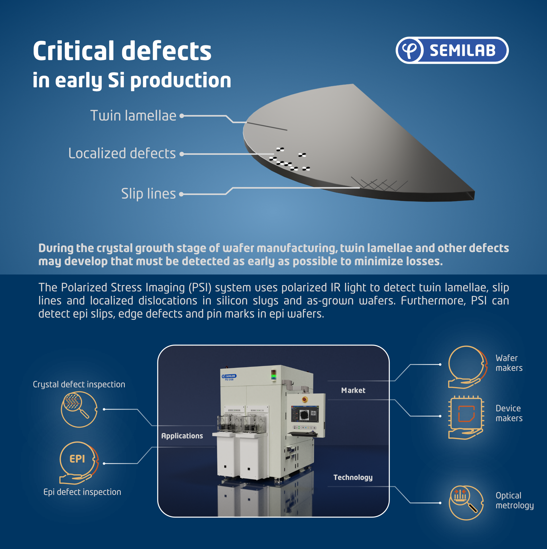
During the crystal growth stage of wafer manufacturing, twin lamellae and other defects may develop that must be detected as early as possible to minimize losses.
The PSI system uses polarized IR light to detect twin lamellae, slip lines and localized dislocations in silicon slugs and as-grown wafers. Furthermore, PSI can detect epi slips, edge defects and pin marks in epi wafers.
If you want to know more about the SEMILAB PSI product family, keep reading HERE!