August 25, 2026
Contact us for Information and Pricing
Get expert advice and tailored solutions for your research needs
Semilab delivers high-precision characterization tools for R&D in Material and Life Sciences, supporting innovation from nanotechnology to biomedical applications.
Semilab has a strong scientific background and a long history of excellent cooperation with academic customers to develop tailored solutions for R&D applications in the semiconductor, photovoltaic and flat panel display industries, thin film research, materials science, and related scientific disciplines.
Material Science
Compact, lab-grade tools for precise electrical resistivity measurement in semiconductor and materials research
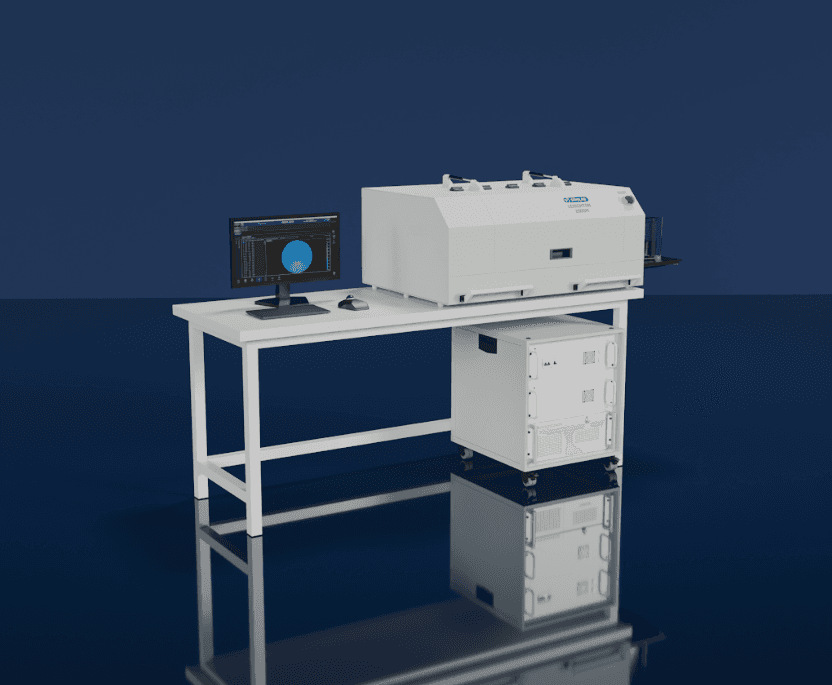
Non-contact, high-sensitivity mapping
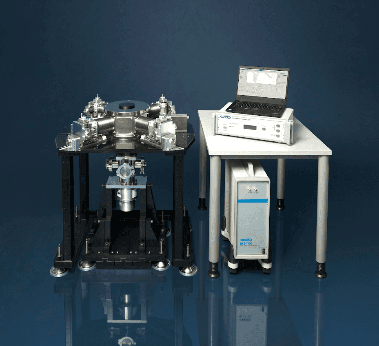
Advanced impurity characterization tools
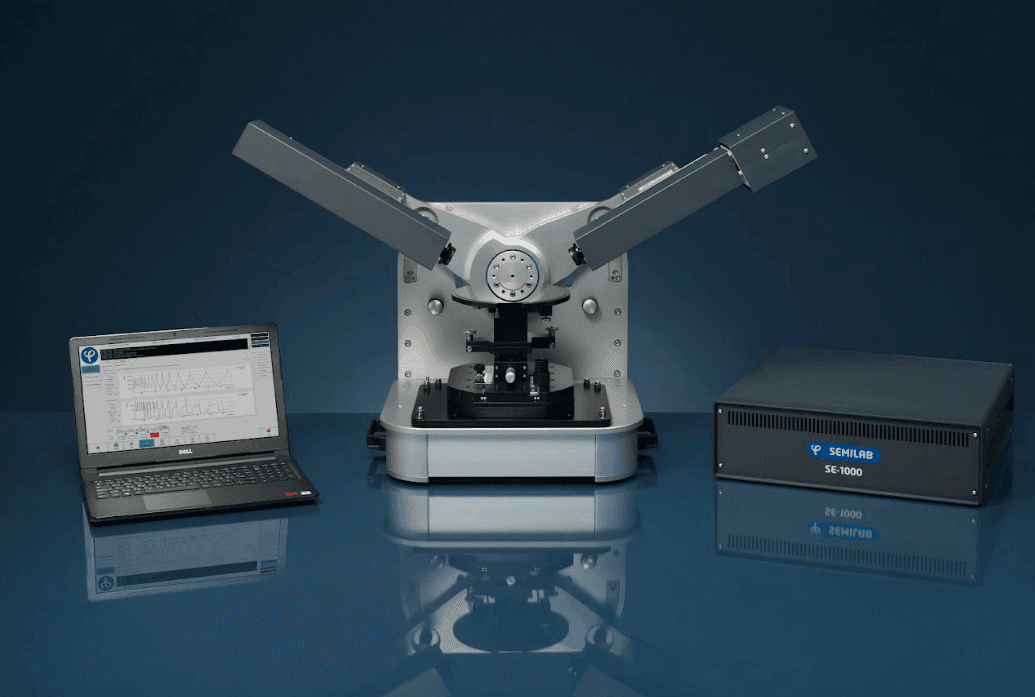
Accurate thin film analysis
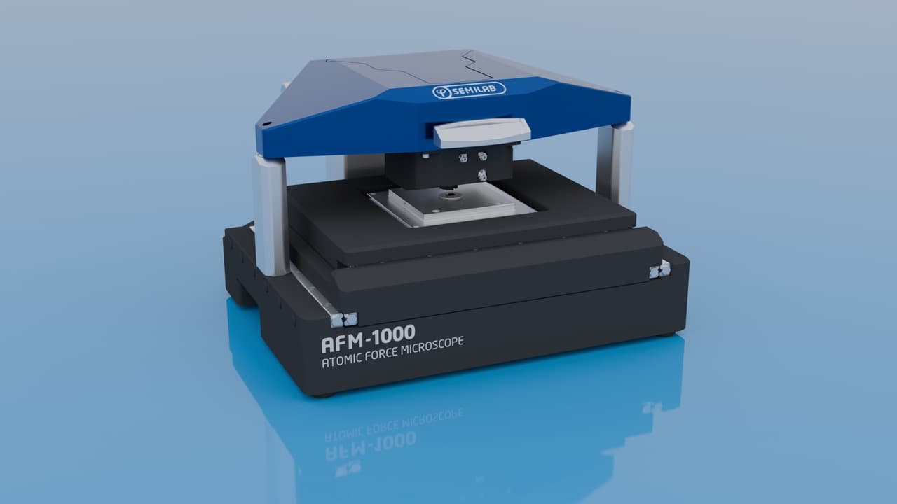
Precision texture and topography mapping
Life Science
Interviews, tips, guides, industry best practices, and news
Read our latest publications
Author: Laszlo Makai, Csaba Balogh, Peter Basa, Jonas Haunschild
Topic: Ellipsometry; Photovoltaics; Monocrystalline textured; TOPCon
Author: Oleg Rusch, Julien Körfer, Boglárka Dikó, Zsófia Kiss, Attila Sütő, Emeric Balogh
Topic: trench MOSFET; OCD; critical dimension metrology; ellipsometry; reflectometry
Author: Zsombor Pap, Bálint Fodor, Julien Körfer, Mathias Rommel, László Makai
Topic: spectroscopic ellipsometry; thin oxide layer measurements; backside reflection; brewster’s angle