
IEEE Photovoltaic Specialists Conference, IEEE NewYork 2000.) p 99.2000
Lifetime mapping of Si Wafers by an Infrared Camera
Author: M. Bail, J. Kentsch, R. Brendel, M. Schulz
Topic: carrier lifetime; infrared camera
Read publication
Contact us for Information and Pricing
Get expert advice and tailored solutions for your research needs
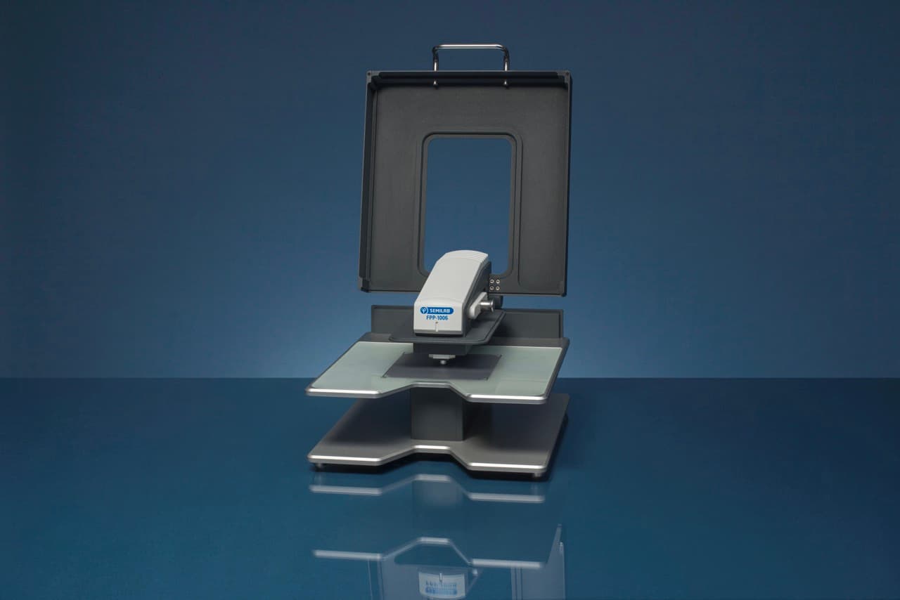
• 6-electrode contact probe eliminating contact resistance effects
• Measurement Principle:
The four point probe (4PP) is a widely used contact technique for monitoring of doping density, resistivity or emitter sheet resistance values. The separation of voltage and current electrodes eliminates the effect of contact resistance from the measurement result. The used voltage is limited so in the high resistivity range the measurable current is getting very small which sets a limitation for the measurement. With our six pin probe (6PP) technique we overcome this problem by using two additional pins to suppress the measurement noise as much as possible.
• High measurement accuracy and excellent repeatability
• Absolute reference measurement technique with no need for calibration
• Fast, easy operation with clear graphical user interface
• Durable probe tips with high longevity under normal use
• Versatile: Can handle a wide range of materials including Si wafers, solar cells, metals, TCOs, and other thin film layers
FPP-1006 Four-Point Probe Measurement